The Semiconductor test board market is one of our specialty, for that market we develop and invest on dedicated technology (eg: jumbo sizes, finishes…)
These boards are called : Test Equipment Load Board, Interface Board, DUT (Device Under Test) board, ATE (Automatic Test Equipment) Board, Probe Card, Socket Board. All these PCB requiere dedicated technology we can provide in short leadtime.
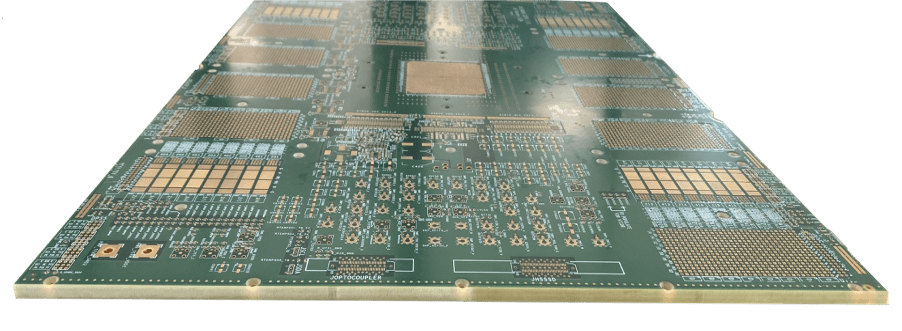
View of a typical Load Board as we supply them (without components):
For that kind of boards we can go up to the following parameters (in some cases it can go higher with some constraints) :
< 50 layers
6,54mm maximum thickness
675X550mm circuit size
3µm à 400µm base copper thickness
50um/50um track and gap
NPTH Socket guide pin alignment +/-20µm
Available in QTA, short production leadtime (few working days)
Dedicated electrical test parameters
Several surface finishes ( Hardgold, ENIG, ENEPIG, Soft Gold possibl ein combination with Solderable Gold)
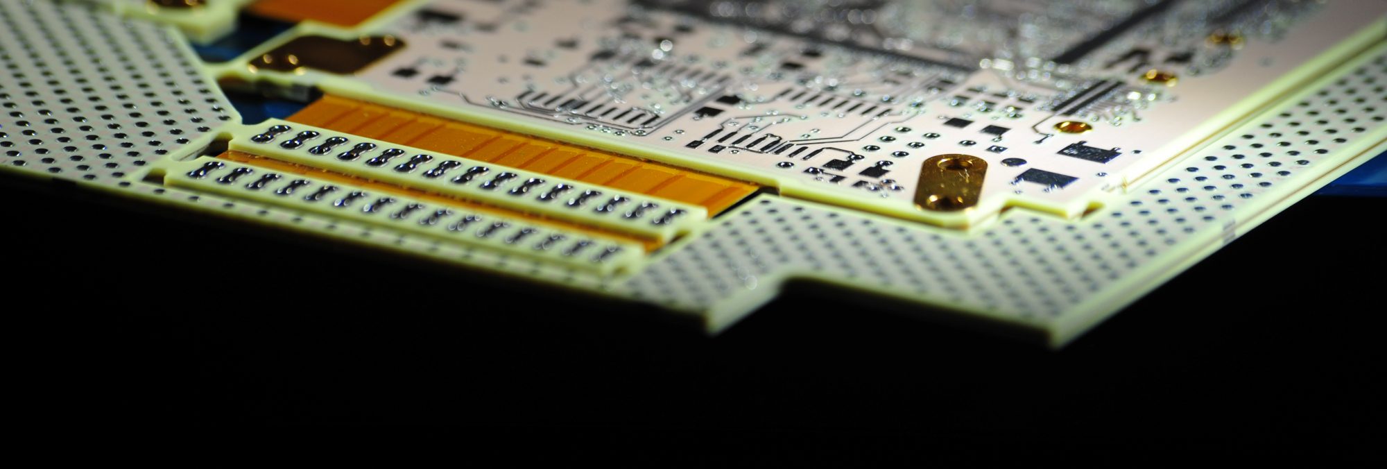
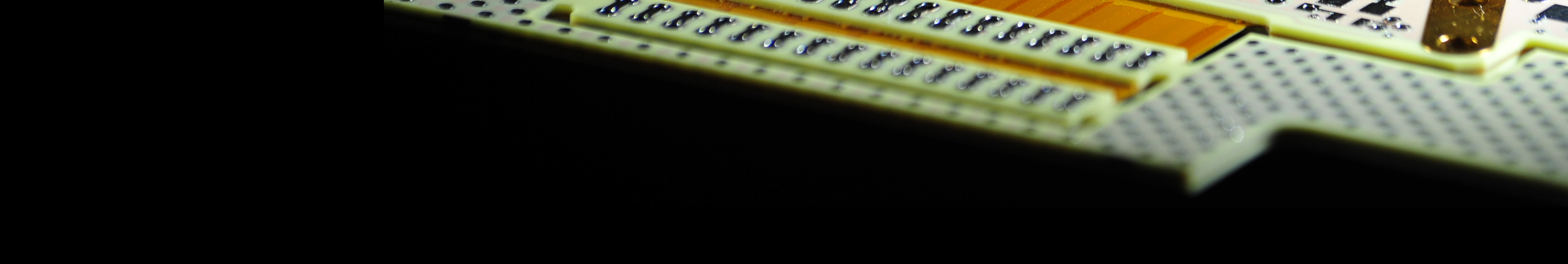
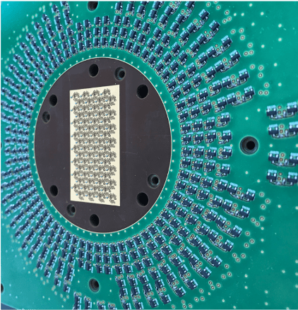
Detailed view of an ATE Board after component assembly (done by external company or by our customers) :
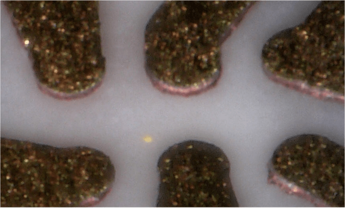
Small overhang area for Electroplated gold pads: